Elon Musk announced on Saturday that Tesla’s “Terafab Project”, a plan to build what he envisions as the world’s largest semiconductor fabrication plant, will launch within seven days.
The problem is that Tesla has absolutely zero experience manufacturing semiconductors, and its track record in the closest comparable venture, building its own battery cells, should give anyone pause.
From battery cells to chips: Tesla’s manufacturing track record
Tesla’s decision to get into chip manufacturing echoes a similar strategic move from six years ago, when the company unveiled its 4680 battery cell at Battery Day in September 2020. Back then, Musk made bold promises: Tesla would build 100 GWh of in-house cell production capacity by 2022, cut battery costs by 56%, and use the savings to deliver a $25,000 electric vehicle.
None of that happened on schedule. The 100 GWh target for 2022 was missed by a wide margin. By early 2025, Tesla’s actual 4680 production was estimated at roughly 20 GWh per year — five years after the announcement and still a fraction of the original 2022 target. The dry electrode process that was central to Tesla’s cost reduction claims proved far more difficult than anticipated. For years, Tesla could only apply it to the anode, while the cathode relied on traditional wet-electrode materials from external suppliers.
The cells themselves didn’t live up to the original promises either. Battery Day claimed the new cell design would deliver 5x more energy, 6x more power, and a 16% range increase. In practice, the 4680 cells went into a single product, the Cybertruck, which has become a commercial failure. Tesla’s 4680 battery supply chain has since collapsed, with supplier L&F Co. writing down its Tesla deal by 99%.
To be fair, Tesla recently achieved some milestones with 4680 cells. The company says it reached the lowest cost per kWh of any cell it produces by the end of 2024, and it has put 4680 cells back in the Model Y. But the broader picture is that Tesla spent six years trying to scale battery cell production — a discipline where it at least had adjacent expertise in battery pack engineering — and still hasn’t delivered on most of its original promises.
Semiconductor fabrication is orders of magnitude more complex.
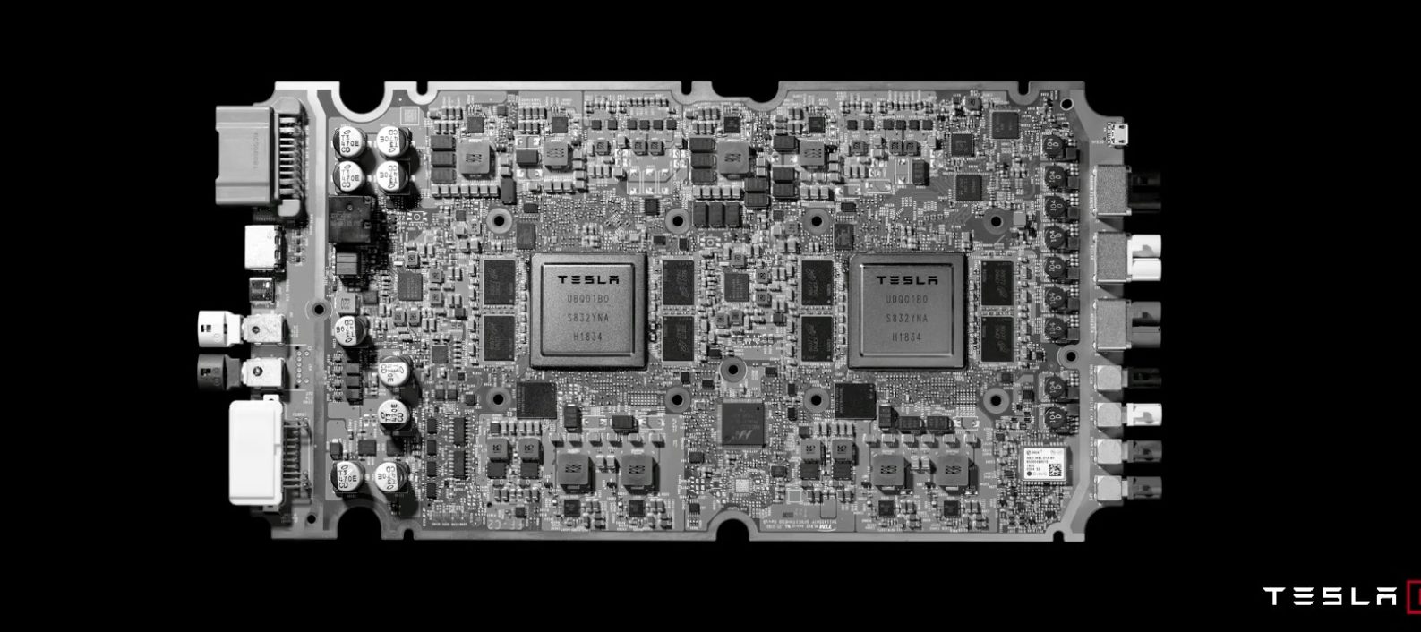
Tesla gutted its own chip talent
The comparison to battery cells is imperfect, of course. Battery cell manufacturing and semiconductor fabrication are fundamentally different disciplines. But that only makes the chip fab challenge harder, because Tesla has even less institutional knowledge in semiconductors than it had in electrochemistry when it launched the 4680 program.
Tesla did build a strong chip design team over the years. The company hired Jim Keller, the legendary chip architect, in 2016, and later brought on Peter Bannon from Apple’s PA Semi team. That team designed Tesla’s custom Autopilot inference chips — HW3 and HW4 — as well as the Dojo training chips. It was a genuine achievement.
But much of that talent is gone. Keller left back in 2018. Ganesh Venkataramanan, who led the Dojo project, departed in late 2023 amid reported issues with the next-generation Dojo 2 chip. Then in August 2025, Musk killed the entire Dojo project, and Peter Bannon — the architect in charge of all custom silicon at Tesla — left the company. About 20 Dojo team members followed Venkataramanan to his new startup, DensityAI, and the remaining workers were reassigned.
That was Tesla’s chip design talent. Chip manufacturing talent is an entirely different workforce — process engineers specializing in lithography, etching, chemical-mechanical planarization, yield management, EUV equipment operation, and dozens of other disciplines that Tesla has never employed. Tesla is now recruiting for these roles, but building a team capable of running a leading-edge 2nm fab from job postings is a far cry from the decades of institutional knowledge that TSMC, Samsung, and Intel have accumulated.
Musk’s cleanroom comments don’t inspire confidence
Musk’s own statements about chip manufacturing suggest he may not fully appreciate the complexity of what he’s proposing. In January, he claimed that the semiconductor industry is “getting clean rooms wrong” and bet that Tesla would build a 2nm fab where he can “eat a cheeseburger and smoke a cigar.”
His argument is that wafers should be fully contained at all times, eliminating the need for a traditional cleanroom environment. Semiconductor experts immediately pushed back. Modern leading-edge fabs operate at ISO Class 1-3 cleanroom standards, where even human breath introduces millions of contamination particles that can destroy chips at the nanometer scale. Smoking a cigar in such an environment would render billions of particles, along with organic contamination that can damage EUV mirrors and fab chemistry.
Even Nvidia CEO Jensen Huang, whose company relies on TSMC for manufacturing, has publicly warned Musk against underestimating the challenge. “Building advanced chip manufacturing is extremely hard,” Huang said at a TSMC event in November 2025. “It is not just build the plant, but the engineering, the science, and the artistry of doing what TSMC does for a living is extremely hard.” Huang went further, telling reporters that matching TSMC’s semiconductor capabilities is “virtually impossible.”
The scale of the challenge
To put the Terafab ambition in perspective: TSMC spent decades and tens of billions of dollars building its manufacturing expertise. Intel, once the world’s leading chipmaker, has struggled for years to regain its manufacturing edge despite having thousands of experienced fab engineers and over $100 billion in investments. Samsung’s foundry business, despite massive investment, still trails TSMC in yield rates at advanced nodes.
Tesla wants to go from zero semiconductor manufacturing experience to running the world’s largest 2nm fab. The company is proposing to combine logic processing, memory storage, and advanced packaging under one roof — something no company, including TSMC, currently does at this scale.
Electrek’s Take
Top comment by CMG30
Elon is going to have to pay through the nose to attract talent. There's no more mission at Tesla, unless you count "Make Elon more money on the stock market" a mission.
Even then, this is a pipe dream. Elon saw how much money NVIDA is making and thought "Why not me?"
We’ve seen this playbook before. Musk announces an impossibly ambitious manufacturing timeline, the stock gets a boost from the excitement, and then reality sets in over the following years as deadlines slip and targets get revised downward.
The 4680 battery cell is the most direct precedent. Six years after Battery Day, Tesla still hasn’t delivered on most of its original promises, and battery cell manufacturing, while difficult, is child’s play compared to leading-edge semiconductor fabrication. The 100 GWh by 2022 target quietly became roughly 20 GWh by 2025. The 56% cost reduction hasn’t materialized at scale. The $25,000 vehicle that was supposed to be enabled by cheap cells still doesn’t exist.
Now Musk is proposing something far more complex, in a field where Tesla has no manufacturing experience, with a team he largely gutted over the past two years, while making comments about smoking cigars in the fab that suggest he doesn’t take the technical challenges seriously. Jensen Huang, who knows more about the semiconductor supply chain than almost anyone alive, is telling him it’s “virtually impossible”, and Huang has every incentive to want more chip production capacity in the world.
Tesla designing its own chips was a smart strategic move that paid off with capable Autopilot hardware. But designing chips and manufacturing them are entirely different things. We’d love to be proven wrong, but the evidence strongly suggests that Terafab will follow the same pattern as 4680: bold promises, years of delays, and results that fall well short of what was originally claimed.
FTC: We use income earning auto affiliate links. More.


Comments